
Christmas Star 2025 [250179]

This project is primarily focused on the PCB design, a perfect 5 pointed star. The schematic is fairly standard, a microcontroller sends data to 20 5 mm digital RGB LEDs connected in series. Through three little push buttons the pattern of the LEDs can be set. To avoid solder pads of through hole components ruining the appearance of the front of the star all components, except the LEDs, are SMD and mounted on the bottom side.
It’s never too soon to start a Christmas project, especially when software is involved. This is a classic 5-pointed star shaped PCB with 20 5mm digital RGB LEDs controlled by a microcontroller. Power supply is 5 V.
The circuit
The circuit
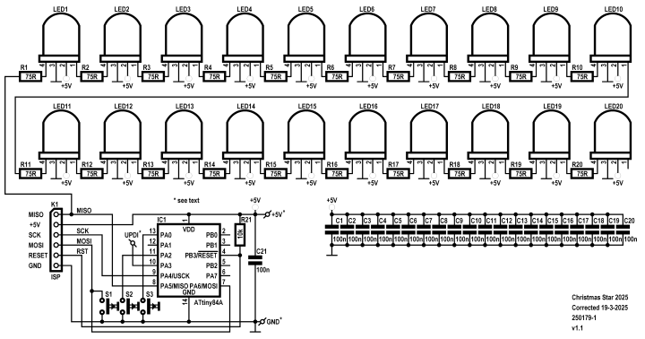
Fig. 1 Schematic of the Christmas Star 2025 (250179-1 v1.1)
The minimum number of LEDs needed to position them in a clear star like shape is 20. A microcontroller from the ATtiny series of Microchip is selected to control the LEDs: a ATtiny84A (IC1) in a 14-pin SOIC package. The Internal 8 MHz RC-oscillator is used as system clock. The microcontroller is In-System Programmable. A 6 pin SMD header with a 0.05” spacing (K1) is place next to the IC and connected to the SPI port, MISO, MOSI, SCK, Reset, +5V and ground. This microcontroller has 8 kByte of flash memory which is enough to program a large variety of patterns. I/O PA5 (is also MISO) is set as output and connected to the first LED. Three very small buttons are available to set the patterns of the LEDs and their properties. The data inputs of the LEDs are connected through 75 Ω resistors, as is recommended in the datasheet. Since the LEDs are in very close proximity of each other they are not strictly necessary and can be replaced by a solder bridge, the two pads are close enough, instead of placing small 0603 resistors. The power supply of each LED is decoupled with 100 nF. Resistors and capacitors are 0603 SMD’s but the are still solderable by hand with a soldering iron with a fine tip. The 5 mm WS2812D-F5 LEDs have two versions. The first is shaped like other standard 5 mm LEDs (almost 9 mm high). The other shape is called straw hat and about 5 mm high. However, while testing the software in combination with the latter shape the mix of the colors is not great, the package is too clear. Even at a distance the three individual LEDs inside the package can clearly be seen and the three are located in the same half of the package. So, the standard shaped version is used in the prototype, the package is more diffused. Before placing the LEDs have a look at the difference of the two types, and decide what version is your preferred one.
In case the 8 kByte of flash memory isn’t enough a newer ATtiny series with more flash memory has types also available in the same 14-pin SOIC package. For instance the ATtiny1604-SSN has 16 kByte and the ATtiny3224-SSU 32 kByte. Of coarse these are also In-System Programmable, but differently. By using a Single-Pin Unified Program and Debug Interface (UPDI) only three connections need to be made to an external programmer.K1 is not needed if one of these types is used. To use UDPI three wires can be connected to solder pads next to IC1: UPDI, GND and +5V. On the internet information can be found how to use USB to serial chips like a FT232 or CH340 as a programmer by connecting Tx and Rx by a resistor or diode. Both these microcontrollers have UPDI connected to pin 10 (14-Pin SOIC package only). Be careful with static charges when soldering a wire to the UPDI pad, it is directly connected to IC1 Also if a soldering station is not grounded the internal mains filter can cause half the mains voltage to be present on the tip of the soldering iron. Ground the soldering iron, especially when the circuit is still connected tot the programmer and/or power supply.
Internally there’s a pull-up resistor on the Reset pin of the ATtiny84A. In the datasheet however it’s stated: Pull-Up resistor on the dW/(RESET) line must be in the range of 10k to 20 kΩ. However, the pull-up resistor is optional. When testing PCB design 1.0 sometimes programming using an AVRISP Mk2 strange errors occurred. After connecting a 10 kΩ pull-up resistor (R21 on PCB v1.1) to the reset pin programming of the microcontroller worked without problems. In the datasheet of the ATtiny3224: AVR devices feature an internal pull-up resistor on the RESET pin, and an external pull-up resistor is usually not required. In the datasheet of the ATtiny1604 there’s no mentioning of this. So on PCB v1.1 there’s no external pull-up resistor connected to the Reset/UPDI pin (also PA0 for these two microcontrollers).
PCB
The 20 5 mm RGB LEDs are placed in such way when drawing a line through the center of the LEDs the same star shape is created as the outline of the PCB. Although, during manufacturing of the PCB a tiny bit of the points of the PCB can be cut off by the milling process. The diameter of the flange of the round LEDs is 5.8 mm in diameter. A small flat piece indicates pin number 1, the data output of the digital LED. To make the front surface of the PCB of the star as evenly white as possible no reference text is placed next to the LEDs and the shape of the footprint is not visible. Except for the LEDs all parts are SMD. To indicate pin1 of the LEDs the solder pad for this pin is rectangular, this is where the flat side of the flange must be located. The other three pads are rounded. The number of the LEDs is the same as the number of the decoupling capacitor next to it. On the bottom side all five tips have small area on which a piece of wire can be soldered. This way a small hook can be added to place the star on or in a Christmas tree or two sturdy wires as a foot to place the star on a flat surface.
Construction
All parts can be soldered by hand using a soldering iron with a fine tip and 0.35 mm solder (or thinner). Start with the smallest 0603 resistors and capacitors. Put a little solder on one pad of each resistor and capacitor. Place each component with tweezers on the PCB and solder the component side where the soldered pad is. Then solder the other side and solder the first side properly. Be careful not to use too much solder. Next do the same with the 3 switches, IC1 and 6-way pin header. To solder the IC first put solder on one pad and place the IC and solder that pin to the PCB while pressing the IC onto the PCB without shifting it. Look if it’s placed symmetrically on the footprint. Then solder the opposite pin on the other (so first pin 1 and then pin 8, or first pin 7 and then 14). All pads of the SMD components footprints are extended a little to make soldering by hand easier and spread the solder better on the pads to prevent to much will be used. Finally the LEDs can be soldered. By gently wriggling the pins they will fit through the holes of the pads, but better is to cut them just above the small widening.
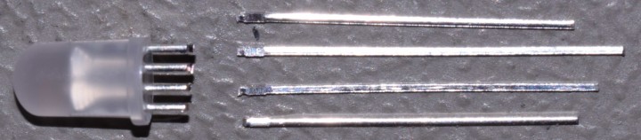
Fig. 2 Leads cut off. The top lead in the photo is pin 1. The flange is partially missing here.
The remaining length of the pins is still more than enough to protrude on the bottom side and be soldered. The flat side of the flange of the LED is pin 1. This indicated by a rectangular pad. The other three pads are rounded. When placing the LEDs check each LED if the orientation is correct and double check after placing them all. Then solder only pin 1 of each LED. Check if each one is placed completely flat against the PCB and correct the ones that are not. Then solder the other leads.
A 5 V power supply could be connected to a second SIL socket to power the Christmas Star through the ISP connector K1. The +5V and ground pin of K1 have text next to them. But a more stable way is to solder two wires to the pads next to IC1.

Fig. 3 Front view of the finished Christmas Star 2025 (PCB 250179-1 v1.0)The minimum number of LEDs needed to position them in a clear star like shape is 20. A microcontroller from the ATtiny series of Microchip is selected to control the LEDs: a ATtiny84A (IC1) in a 14-pin SOIC package. The Internal 8 MHz RC-oscillator is used as system clock. The microcontroller is In-System Programmable. A 6 pin SMD header with a 0.05” spacing (K1) is place next to the IC and connected to the SPI port, MISO, MOSI, SCK, Reset, +5V and ground. This microcontroller has 8 kByte of flash memory which is enough to program a large variety of patterns. I/O PA5 (is also MISO) is set as output and connected to the first LED. Three very small buttons are available to set the patterns of the LEDs and their properties. The data inputs of the LEDs are connected through 75 Ω resistors, as is recommended in the datasheet. Since the LEDs are in very close proximity of each other they are not strictly necessary and can be replaced by a solder bridge, the two pads are close enough, instead of placing small 0603 resistors. The power supply of each LED is decoupled with 100 nF. Resistors and capacitors are 0603 SMD’s but the are still solderable by hand with a soldering iron with a fine tip. The 5 mm WS2812D-F5 LEDs have two versions. The first is shaped like other standard 5 mm LEDs (almost 9 mm high). The other shape is called straw hat and about 5 mm high. However, while testing the software in combination with the latter shape the mix of the colors is not great, the package is too clear. Even at a distance the three individual LEDs inside the package can clearly be seen and the three are located in the same half of the package. So, the standard shaped version is used in the prototype, the package is more diffused. Before placing the LEDs have a look at the difference of the two types, and decide what version is your preferred one.
In case the 8 kByte of flash memory isn’t enough a newer ATtiny series with more flash memory has types also available in the same 14-pin SOIC package. For instance the ATtiny1604-SSN has 16 kByte and the ATtiny3224-SSU 32 kByte. Of coarse these are also In-System Programmable, but differently. By using a Single-Pin Unified Program and Debug Interface (UPDI) only three connections need to be made to an external programmer.K1 is not needed if one of these types is used. To use UDPI three wires can be connected to solder pads next to IC1: UPDI, GND and +5V. On the internet information can be found how to use USB to serial chips like a FT232 or CH340 as a programmer by connecting Tx and Rx by a resistor or diode. Both these microcontrollers have UPDI connected to pin 10 (14-Pin SOIC package only). Be careful with static charges when soldering a wire to the UPDI pad, it is directly connected to IC1 Also if a soldering station is not grounded the internal mains filter can cause half the mains voltage to be present on the tip of the soldering iron. Ground the soldering iron, especially when the circuit is still connected tot the programmer and/or power supply.
Internally there’s a pull-up resistor on the Reset pin of the ATtiny84A. In the datasheet however it’s stated: Pull-Up resistor on the dW/(RESET) line must be in the range of 10k to 20 kΩ. However, the pull-up resistor is optional. When testing PCB design 1.0 sometimes programming using an AVRISP Mk2 strange errors occurred. After connecting a 10 kΩ pull-up resistor (R21 on PCB v1.1) to the reset pin programming of the microcontroller worked without problems. In the datasheet of the ATtiny3224: AVR devices feature an internal pull-up resistor on the RESET pin, and an external pull-up resistor is usually not required. In the datasheet of the ATtiny1604 there’s no mentioning of this. So on PCB v1.1 there’s no external pull-up resistor connected to the Reset/UPDI pin (also PA0 for these two microcontrollers).
PCB
The 20 5 mm RGB LEDs are placed in such way when drawing a line through the center of the LEDs the same star shape is created as the outline of the PCB. Although, during manufacturing of the PCB a tiny bit of the points of the PCB can be cut off by the milling process. The diameter of the flange of the round LEDs is 5.8 mm in diameter. A small flat piece indicates pin number 1, the data output of the digital LED. To make the front surface of the PCB of the star as evenly white as possible no reference text is placed next to the LEDs and the shape of the footprint is not visible. Except for the LEDs all parts are SMD. To indicate pin1 of the LEDs the solder pad for this pin is rectangular, this is where the flat side of the flange must be located. The other three pads are rounded. The number of the LEDs is the same as the number of the decoupling capacitor next to it. On the bottom side all five tips have small area on which a piece of wire can be soldered. This way a small hook can be added to place the star on or in a Christmas tree or two sturdy wires as a foot to place the star on a flat surface.
Construction
All parts can be soldered by hand using a soldering iron with a fine tip and 0.35 mm solder (or thinner). Start with the smallest 0603 resistors and capacitors. Put a little solder on one pad of each resistor and capacitor. Place each component with tweezers on the PCB and solder the component side where the soldered pad is. Then solder the other side and solder the first side properly. Be careful not to use too much solder. Next do the same with the 3 switches, IC1 and 6-way pin header. To solder the IC first put solder on one pad and place the IC and solder that pin to the PCB while pressing the IC onto the PCB without shifting it. Look if it’s placed symmetrically on the footprint. Then solder the opposite pin on the other (so first pin 1 and then pin 8, or first pin 7 and then 14). All pads of the SMD components footprints are extended a little to make soldering by hand easier and spread the solder better on the pads to prevent to much will be used. Finally the LEDs can be soldered. By gently wriggling the pins they will fit through the holes of the pads, but better is to cut them just above the small widening.
Fig. 2 Leads cut off. The top lead in the photo is pin 1. The flange is partially missing here.
The remaining length of the pins is still more than enough to protrude on the bottom side and be soldered. The flat side of the flange of the LED is pin 1. This indicated by a rectangular pad. The other three pads are rounded. When placing the LEDs check each LED if the orientation is correct and double check after placing them all. Then solder only pin 1 of each LED. Check if each one is placed completely flat against the PCB and correct the ones that are not. Then solder the other leads.
A 5 V power supply could be connected to a second SIL socket to power the Christmas Star through the ISP connector K1. The +5V and ground pin of K1 have text next to them. But a more stable way is to solder two wires to the pads next to IC1.
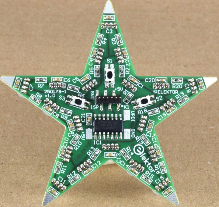
Fig. 4 View on the back of the finished Christmas Star 2025 (PCB 250179-1 v1.0)
Software and programming
The software was developed for the ATtiny84A using Bascom-AVR 2.0.8.6. An additional license is needed to develop software for the newer ATtiny series (like the 1604 and 3224).
The ATtiny84A can be programmed through ISP. A 6-way pin header with 1.27 mm (0.05”) spacing must be soldered onto the PCB to program the ATtiny84A. An adapter can be made to connect a AVRISP MkII or similar in-circuit programmer. A 1x6 pin socket with 1.27 spacing can be soldered directly to a 2.54 mm pin 2x3 pin header with 2.54 mm spacing without the need of having to use additional wiring.
Fig. 5 Self-made adapter to connect an ISP programmer like AVRISP MkII. Handle with care!
Be careful! The pins of the small SIL header are fragile and break easily, I broke two of them during the development of the software. Maybe glue struts between the two headers so they can’t move and thus relieve any strain on the solder joints and pins. Perhaps type DS1065-07-1*6S8BV of Connfly is more solid. Also type M50-3030642 from Harwin looks less fragile.
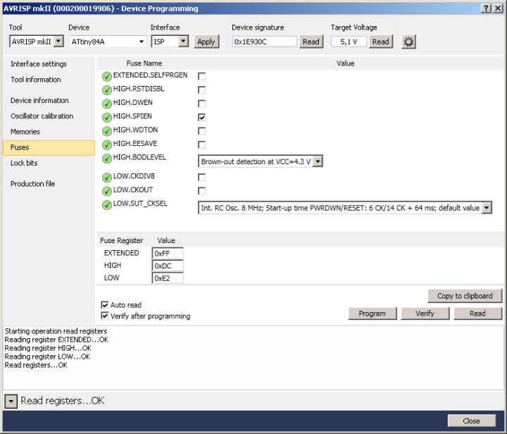
Fig. 6 Fuse settings for the ATtiny84A.
The screen dump above shows the correct fuse settings for the ATtiny84A. For the Rainbow instructions to work properly the clock of the microcontroller must be 8 MHz. So fuse ‘Divide Clock by 8’ (CKDIV8) must be turned off. Something else. While connecting the PCB to different power supplies sometimes the LED’s stayed off. Pushing buttons until some LEDs froze, and then turning the power supply off and on again seemed to solve the problem. This happened with Bown-out detection off. Obviously at power-up the EEPROM data is not read correctly. I set the fuse for the Brown-out detection to 4.3 V. This seems to have solved it. Maybe a check after reading the EEPROM data is missing, to be sure that all three bytes for EE_ Pattern (valid data is 0 to 7), EE_Delaynumber (valid data is 1 to 10) and EE_Levelnumber (valid data is 1 to 10) have numbers within the used range.
About the example software in Bascom AVR (250179-11.zip). Switches S1, S2 and R3 control the pattern of the LEDs, delay of changes in the pattern and maximum brightness respectively. 7 Patterns are possible:
Pattern
- Color of all LEDs change randomly
- All LEDs are white but brightness changes randomly
- All LEDs are red
- All LEDs are green
- All LEDs are blue
- All LEDs are white
- Colors red, green, blue, yellow, magenta and cyan shift outward, from the 5 inner LEDs to the 10 middle LEDs to 5 LEDs in the tips
- 4 LEDs in each tip have the same color, each tip a different color. 5 colors (red, green, cyan, yellow and magenta) rotating clockwise.
After pushing one of the switches 10 LEDs in the middle of the 5 tips are used to indicate the new setting. Color white for S1 (pattern), color yellow for S2 (delay) and color magenta for S3 (brightness). The number of LEDs that blink twice show the number of the setting. S1: 1 LED blinking is pattern 0.
To keep tracks in the PCB design as short as possible pin 5 of port A was used to control the LEDs. But this is also MISO. So after programming the microcontroller the LEDs are set to random data and the power supply current is higher than the maximum in normal operation (defined by the software used). After programming disconnect the programmer and turn the power supply off and on again. The circuit will work normally now.
Ports used for the LEDs, S1, S2 and S3:
84A 1604/3224
LED1 PA5 PB1
S1 PA6 PB2
S2 PA2 PA1
S3 PA0 PA3
This means in case one of the newer ATtiny’s is used the software must adapted/changed since different ports are connected to the individual pins!
Feel free to develop other patterns and software and share it here.
A few properties
Power supply voltage is 5V. Absolute maximum is 5.3 V, defined by the LEDs. At the current maximum brightness setting (110 for each color, maximum for the WS2812D-F5 is 255 per color) the maximum power supply current is about 300 mA. But, when programming the microcontroller the LED’s will receive random data and the current is a lot higher, close to 700 mA. The size of the PCB according to the design is horizontal from tip to tip 69.30 mm and vertically from tip to tip 65.91. Due to milling the size of the manufactured PCB can be a little smaller, our prototype is about 65.8 x 62.6 mm.
Here are a few photos with different patterns. The photos don’t do the brilliance of the LEDs justice. Current of the LEDs was set very low to prevent overexposing the camera. Otherwise all LEDs would simply appear white.
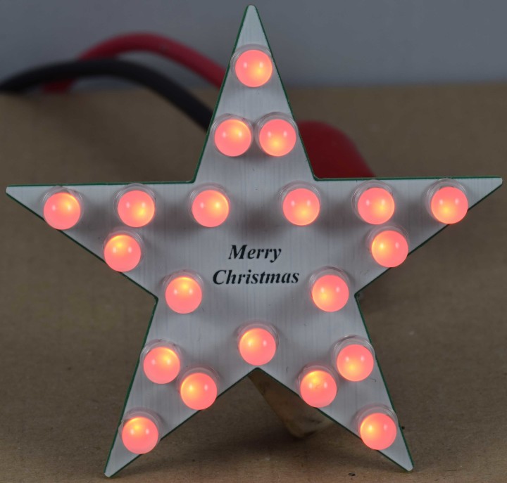
Fig. 7 Pattern 2, all LEDs red only.
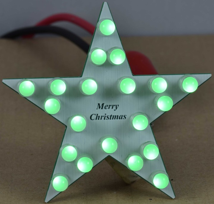
Fig. 8 Patern 3, all LEDs green only.
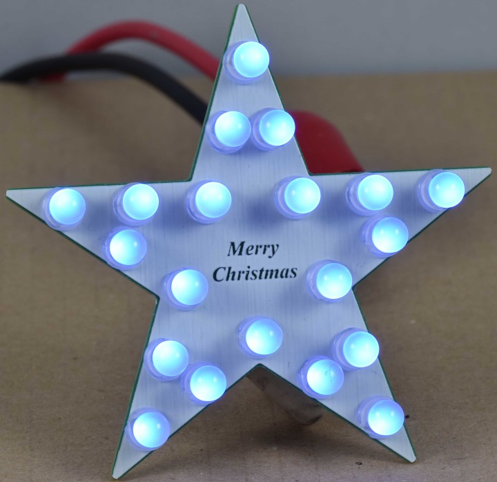
Fig. 9 Pattern 4, all LEDs blue only.

Fig. 10 Pattern 0, all LEDs have random changing colors .

Fig. 11 Pattern 6, 7 colors shift outwards. LEDs in the same position in each tip have the same color.

Fig. 12 Pattern 7. 5 colors rotate clockwise, 4 LEDs in each tip have the same color.
Bill of materials 250170-1 v1.1
Resistor
R1-R20 = 75 Ω, 100 mW, SMD 0603
R21 = 10 kΩ, 100 mW, SMD 0603
Capacitor
C1-C21 = 100 nF, 50 V, X7R, SMD 0603
Semiconductor
LED1-LED20 = WS2812D-F5 Worldsemi, through hole, D 5mm
ATtiny84A, SMD SOIC-14
Other
K1 = 1x6 pin header, SMD straight, pitch 1.27 mm (0.05”), M50-3630642 Harwin or DS1031-03-1*6P8BS311-3A Connfly
K1 = 1x6 pin socket, pitch 1.27 mm, M50-3030642 Harwin or DS1065-01-1*6S8BV Connfly or DS1065-07-1*6S8BV Connfly
S1, S2, S3 = Tactile switch, SPST-NO, SMD, KMR221G LFS C&K Components
2x3 pin header pitch 2.54 mm (0.1”), for making the ISP adapter with 1x6 pin socket
Misc.
PCB 250179-1 v1.1
PCB – Overlay and copper

Fig. 13 Top overlay of PCB 250179-1 v1.1 of the Christmas Star 2025
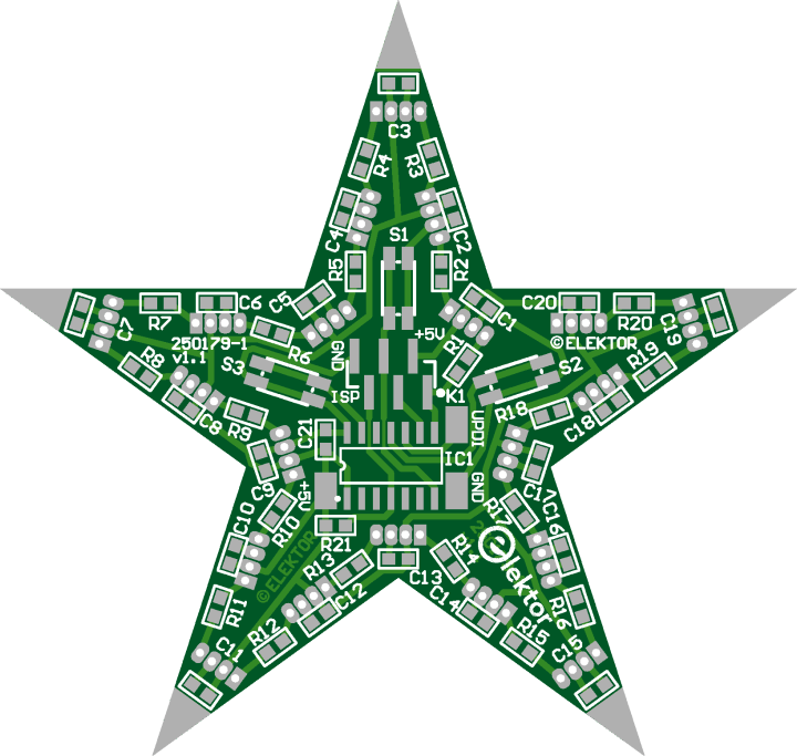
Fig. 14 Bottom overlay of PCB 250179-1 v1.1 of the Christmas Star 2025

Fig. 15 Copper on top of PCB 250179-1 v1.1 of the Christmas Star 2025

Fig. 16 Copper on bottom of PCB 250179-1 v1.1 of the Christmas Star 2025
Discussion (0 commentaire(s))